Dynamic random-access memory
|
COMPUTER MEMORY
Dynamic random-access memory
DRAM
| |||||||||||
 i i
| |||||||||||
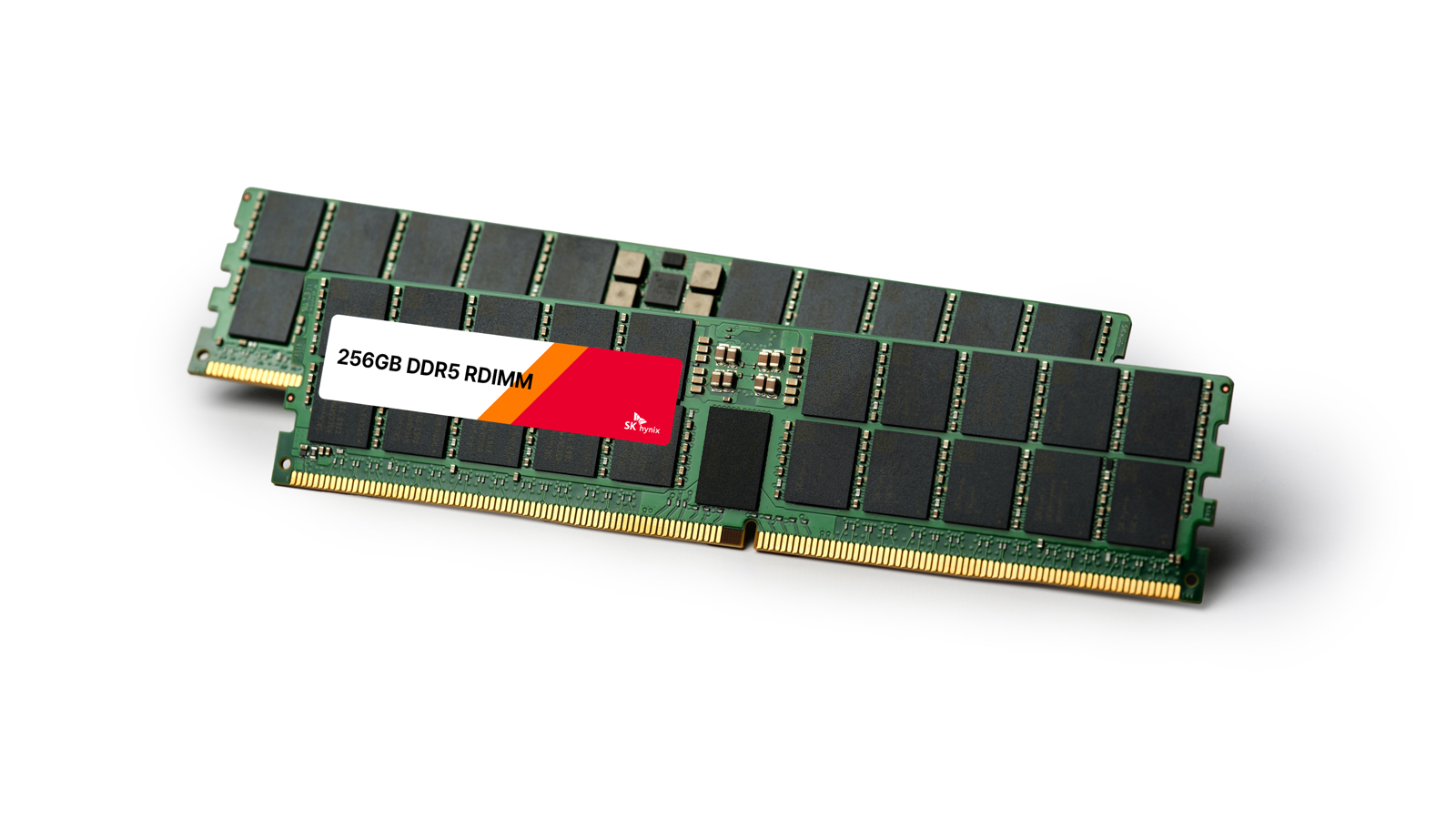
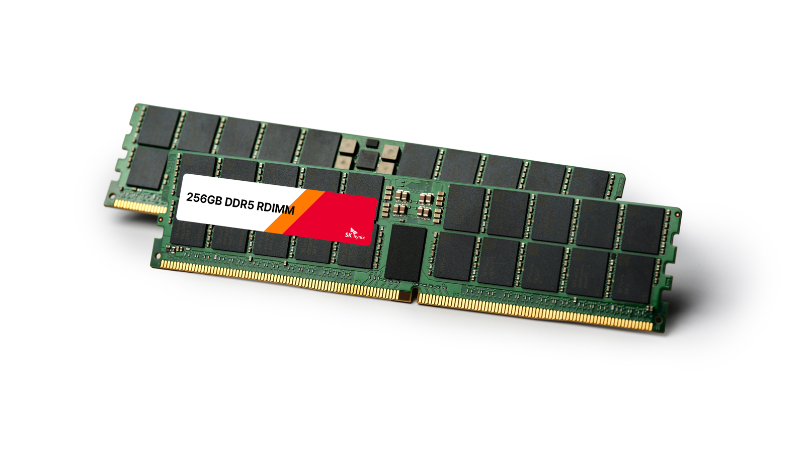
A 256GB DDR5 module from SK hynix, built from 32-gigabit chips — the form in which DRAM is sold for desktop and server computers
| |||||||||||
| Type | Volatile semiconductor memory[1] | ||||||||||
|---|---|---|---|---|---|---|---|---|---|---|---|
| Invented | 1966; patented 1968[2] | ||||||||||
| Inventor | Robert H. Dennard, at IBM[2] | ||||||||||
| Cell | One transistor and one capacitor[1][3] | ||||||||||
| First product | Intel 1103, October 1970[4] | ||||||||||
[ More details ▾ ]
| |||||||||||
Dynamic random-access memory, almost always shortened to DRAM, is the kind of memory a computer uses as its working space while it is running. It holds the operating system, the programs in use and the data they are handling, and it gives up all of that the moment the power goes off. Every desktop computer, laptop, phone, games console, car and data-centre server contains DRAM, and for most of them it is the second most expensive component after the processor.[1][9]
The name describes how it works. Each bit is stored as an electrical charge on a tiny capacitor, and that charge leaks away within a fraction of a second. To keep the data alive, the chip must read every cell and write it back thousands of times a second, a process called refresh. Memory that must be topped up like this is called dynamic, in contrast to the static memory used for processor caches, which holds its contents for as long as the power is on.[2][9]
DRAM was invented in 1966 by Robert Dennard, an engineer at IBM, who worked out that a single transistor and a single capacitor were enough to store one bit.[2] That was a drastic simplification: the memory cells of the day used six transistors each. The first commercial chip, Intel's 1103 of 1970, held 1,024 bits and cost about a cent per bit, cheap enough to displace the magnetic core memory that computers had used until then.[10][4] Modern chips built on the same basic cell hold tens of billions of bits.[11]
Because DRAM is a commodity — one maker's DDR5 chip is interchangeable with another's — the business has always run in violent cycles of glut and shortage. Three companies now supply almost the whole market: Samsung Electronics, SK hynix and Micron Technology together took about 90% of DRAM revenue in the first quarter of 2026.[8] The artificial-intelligence build-out that began in 2023 pushed the industry into the sharpest shortage in its history, and contract prices for ordinary DRAM roughly doubled in a single quarter in early 2026.[8]
1 How it works✎
1.1 The cell✎
A DRAM chip is a grid of cells, each holding one bit. A cell has just two parts: a capacitor, which stores an electrical charge, and a transistor, which acts as a switch controlling access to it. A charged capacitor is read as a 1 and a discharged one as a 0.[1][3]
This is what made Dennard's design so important. Static memory needs six transistors to hold a bit, so a DRAM cell takes far less room on the silicon and costs far less to make. The penalty is that a capacitor is a leaky container, while a static cell is a latch that simply stays where it is put.[9][12]
1.2 Refresh✎
Charge escapes a DRAM capacitor through several paths at once, and a cell left alone will lose its contents in well under a second.[13] The chip therefore works through its rows continuously, reading each one and writing it straight back. The DDR3 and DDR4 standards guarantee that a cell keeps its value for at least 64 milliseconds, so the whole array must be refreshed within that window. A refresh command is issued on average every 7.8 microseconds.[13][3]
Heat makes leakage worse, and above 85 °C the interval is halved.[13] Denser chips have tightened the budget further: Micron's 16-gigabit DDR5 parts must be refreshed within 32 milliseconds rather than 64.[11] Refresh is pure overhead — while a bank is being refreshed it cannot serve the processor — so DDR5 added a mode that refreshes one bank at a time instead of stalling the whole device, which Micron measures as worth a 6% to 9% gain in system throughput.[14]
1.3 Reading a cell destroys it✎
Reading DRAM is not a passive act. Opening the transistor lets the capacitor's charge spill onto a shared wire called a bit line, which wipes out the stored value. A circuit called a sense amplifier detects the resulting tiny change in voltage, decides whether it represents a 1 or a 0, and immediately writes the value back into the cell.[3][12] Cross-coupled differential sense amplifiers of this kind have been part of DRAM design since the early 1970s.[12]
1.4 Rows, columns and banks✎
Cells sit at the crossing points of horizontal wires called word lines and vertical wires called bit lines.[3] Reading anything therefore happens in three steps: activate a row, which copies the entire row into the sense amplifiers; read or write the column the processor actually wants; then precharge, closing the row again.[15]
This is why the "random access" in the name is a little misleading. If the row a program wants is already open, the data comes back quickly; if a different row is open, it must be closed first, which costs considerably more time.[15] Chips are divided into banks, and DDR5 groups them further into bank groups — a 16-gigabit device has 32 banks arranged in eight groups — so that several rows can be open at once and requests can be spread across them.[11][14]
The best-known DRAM timing figure, CAS latency, measures how many clock cycles pass between the request for a column and the data appearing on the pins. It is only meaningful alongside the clock speed, since a faster clock makes each cycle shorter; a DDR5-5600 module rated CL46 and a DDR5-7200 module rated CL58 are closer in real terms than the numbers suggest.[16][11] Overall, DRAM takes roughly 30 to 50 nanoseconds to deliver data that a processor cache can supply in under one.[15]
2 DRAM, SRAM and flash✎
Computers use several kinds of memory because no single technology is fast, dense and cheap at the same time. The three that matter most sit in a clear order.[9][1]
| Technology | Transistors per bit | Speed | Keeps data without power? | Typical use |
|---|---|---|---|---|
| SRAM | 6 | Fastest | No | Processor cache |
| DRAM | 1 (plus a capacitor) | Middle | No | Main memory |
| NAND flash | Shared, stacked in layers | Slowest | Yes | Storage |
Static RAM is built from latches rather than capacitors, needs no refresh and answers in well under a nanosecond, but its six-transistor cell makes it roughly a hundred times more expensive per bit. That confines it to the small caches inside a processor.[9] NAND flash traps charge in an insulating film, so it keeps data with the power off, but writing is slow and each cell wears out with use; it is used for storage rather than working memory.[1] DRAM sits between them, and the gap it fills has proved remarkably durable.
3 History✎
3.1 Invention, 1966–1970✎
Robert Dennard conceived the one-transistor memory cell at IBM's Thomas J. Watson Research Center in 1966. He and IBM received United States patent 3,387,286 for it on 4 June 1968, on an application filed the previous July.[2][10] Dennard later described the essential idea simply: an MOS transistor placed in series with each capacitor could serve as a switch, connecting that capacitor briefly to a data line.[12]
Intel brought semiconductor memory to market first, with the 1103 in October 1970. It stored 1,024 bits using a three-transistor cell proposed by Bill Regitz of Honeywell rather than Dennard's single-transistor design, and at about a cent per bit it was the first chip to seriously undercut magnetic core memory.[10][2] The effect was rapid. By the end of 1971 the 1103 was the best-selling semiconductor device in the world, and within a year roughly 78% of the large mainframe makers in the United States, Europe and Japan had designed it in.[4] Dennard's simpler cell took over as densities rose, and it remains the basis of every DRAM chip made today.[10][3]
3.2 The asynchronous era✎
Early DRAM had no clock. The memory controller pulled control lines up and down and waited a fixed time for an answer, an arrangement that became a bottleneck as processors sped up. Fast page mode, which kept a row open so that further columns could be fetched quickly, was the mainstream design as late as 1994. Extended data out, or EDO, held the output valid a little longer and improved page-mode throughput by about 40%.[17][18]
3.3 Synchronous DRAM and the DDR generations✎
The answer was to give the memory a clock. Synchronous DRAM, or SDRAM, runs in step with the memory controller, which lets it pipeline requests and deliver a burst of data on consecutive cycles. Manufacturers worked through JEDEC, the industry's standards body, from the early 1990s, and JEDEC's SDRAM specification carries a release dated June 1994. The design displaced the older architectures across the PC industry within a few years.[18][19][17]
Every generation since has been an evolution of that idea. Double data rate memory, standardised by JEDEC as JESD79 in June 2000, transfers data on both the rising and the falling edge of the clock, doubling throughput without doubling the clock speed.[20] DDR2 followed, then DDR3, published on 26 June 2007, which ran from 1.5 volts at 800 to 1,600 transfers per second.[21] DDR4 arrived on 25 September 2012, starting at 1.6 billion transfers per second with an initial target of 3.2 billion, and dropped the supply voltage to 1.2 volts.[22][23]
DDR5, published on 14 July 2020, launched at 4.8 billion transfers per second on 1.1 volts, with twice the burst length and twice as many banks. That opening speed was half again as fast as DDR4 managed at the end of its life.[6] It has been revised repeatedly since. A 2024 update raised the ceiling to 8,800 transfers per second and added defences against the Rowhammer attack described below, and the current revision was published in November 2025.[24][25] A successor is being drafted: JEDEC states that DDR6 is in development in its JC-42 committee, though no standard has been published and no official speeds announced.[5]
4 Variants✎
The same cell is packaged very differently depending on what the memory has to do. Three families dominate.
4.1 LPDDR✎
Low-power DDR trades some peak performance for much lower power draw, which is what battery-powered devices need. It is the memory in nearly every smartphone and in most thin laptops. JEDEC published the LPDDR6 standard on 9 July 2025; it splits each channel into two sub-channels, scales voltage and frequency down when demand is light, and can shut one sub-channel off entirely.[26] Samsung's first LPDDR6 parts reach 10.7 gigabits per second per pin and claim about 21% better energy efficiency than the previous generation.[27]
Low-power memory has since escaped the phone. AI servers burn enormous amounts of electricity, and a large share of it goes on memory, so the same parts are now being fitted to data-centre machines in module form.[28]
4.2 GDDR✎
Graphics DDR is tuned the other way: it accepts higher power and latency in exchange for raw bandwidth, because a graphics processor works through very large blocks of data at once. JEDEC published GDDR7 on 5 March 2024, reaching 32 gigabits per second on each pin and up to 192 gigabytes per second per chip. It was the first JEDEC memory standard to use three-level PAM3 signalling, which carries more information per clock edge than a simple on-off scheme.[29] NVIDIA's GeForce RTX 50 series, announced in January 2025, was the first major product line built on it.[30] Not every graphics part is a JEDEC standard: GDDR6X was developed by Micron and NVIDIA together, outside the standards process.[31]
4.3 High Bandwidth Memory✎
High Bandwidth Memory, or HBM, abandons the flat layout altogether. Several DRAM dies are stacked on top of one another and joined by through-silicon vias, vertical wires that run straight through the silicon. The stack then talks to the processor over an interface thousands of wires wide instead of a few dozen. That buys enormous bandwidth at lower power, at the cost of a far harder and more expensive manufacturing process.[32]
SK hynix and AMD built the first through-silicon-via HBM product in 2014.[32] JEDEC standardised HBM3 in January 2022 at up to 819 gigabytes per second per device, and HBM4 on 16 April 2025, which widens the interface to 2,048 bits and reaches up to two terabytes per second and 64 gigabytes in a single stack.[33][34] AI accelerators are limited far more often by how fast they can be fed than by how fast they can calculate. That has made HBM the most valuable product in the memory industry, and SK hynix has led it since the market became important.[35]
5 Memory modules✎
Individual chips are rarely sold on their own. They are mounted on small circuit boards called modules, and the module format determines what a machine can accept.[7]
- DIMM — the long board used in desktops and servers. An unbuffered DIMM wires the controller straight to the chips; a registered DIMM (RDIMM) puts a register in between, which adds about a cycle of delay but lets a machine carry far more memory. A load-reduced DIMM (LRDIMM) adds buffers on the data lines too, for the largest capacities.[7][36][37]
- SO-DIMM — a short module, about 70 millimetres long, for laptops and other cramped machines.[7]
- CAMM2 — a flat module standardised by JEDEC on 5 December 2023, designed to be thinner than a SO-DIMM and to run at higher speeds. One specification covers a DDR5 version for performance laptops and desktops and an LPDDR5X version for thinner machines.[38]
- MRDIMM — a server module that multiplexes two ranks of ordinary DDR5 chips to deliver up to twice the bandwidth. JEDEC set out the programme in July 2024 and published further interface standards in April 2026, with a second generation targeting 12,800 transfers per second.[39][40]
- SOCAMM2 — a compact LPDDR5X module for AI servers, roughly a third the size of an RDIMM, which JEDEC announced in October 2025 and published in June 2026.[28][41]
A separate approach attaches memory over the CXL protocol rather than the usual memory channels. That lets a server add capacity beyond what its processor sockets allow, and lets several machines share a pool of memory. Samsung sells such modules in 128 and 256 gigabyte capacities.[42]
6 Making DRAM✎
Two capacitor designs have shaped the industry: the trench capacitor, dug down into the silicon, and the stacked capacitor, built above the transistor. The stacked approach, which grew out of work by Mitsumasa Koyanagi placing the capacitor over the bit line, is what the surviving manufacturers use.[12]
Shrinking a DRAM cell is harder than shrinking a logic circuit, because the capacitor still has to hold enough charge to be read reliably even as its footprint gets smaller. Makers have answered by building it taller and narrower, and the ratio of height to width now climbs steeply with each generation, which is the main reason DRAM scaling has slowed and costs have risen.[43]
Manufacturers label their processes by generation rather than by any measured dimension. SK hynix and Samsung Electronics count 1x, 1y, 1z, 1a, 1b and 1c within what they call the ten-nanometre class; Micron uses Greek letters, with 1-gamma its sixth such node.[44][45] Extreme ultraviolet lithography, long confined to logic chips, is now used across the leading DRAM nodes; Micron adopted it last, with 1-gamma in 2025.[44][46]
The industry's answer to the scaling problem is to build upwards. SK hynix has named three-dimensional DRAM as the main pillar of its future roadmap, together with a denser cell layout known as 4F² and vertical-gate transistors.[47] Samsung has set out a similar path, with stacked DRAM arriving in the early 2030s.[48]
7 Reliability and security✎
DRAM is not perfectly reliable, and at modern densities it cannot be. Every DDR5 chip therefore carries error-correcting code built into the die itself, which protects blocks of 128 data bits with eight extra parity bits and repairs single-bit errors before the data leaves the chip.[49][11] On-die correction is not the same thing as the error-correcting memory sold for servers, which adds extra chips to a module and protects the whole path between the processor and the memory.[49]
The best-known DRAM weakness is Rowhammer, described in a 2014 paper by Yoongu Kim and colleagues. Because cells are packed so tightly, repeatedly opening and closing one row makes neighbouring rows leak charge much faster than usual, and bits in those rows can flip. The researchers found that as few as 139,000 accesses could produce an error, and that up to one cell in every 1,700 was vulnerable.[3] The attack matters because those neighbouring rows may belong to another program, so an attacker who can only read their own memory may still be able to corrupt someone else's.
Manufacturers first responded with a family of countermeasures marketed as target row refresh, which a 2020 study showed could be sidestepped by hammering several rows at once.[50] JEDEC's more recent answer is Per Row Activation Counting, added to DDR5 in April 2024 and to LPDDR6 in 2025. It counts activations on each individual word line and signals the system to pause traffic when a count runs high.[24][26]
8 The industry✎
DRAM is made by very few companies, because a modern fabrication plant costs tens of billions of dollars and the product is interchangeable between suppliers. In the first quarter of 2026 the market was worth US$97 billion for the quarter alone, split between Samsung Electronics at 38.5%, SK hynix at 28.8% and Micron Technology at 22.4% — nearly 90% between them.[8] A fourth supplier has emerged in China: ChangXin Memory Technologies held roughly 9% of shipments in early 2026 and listed on Shanghai's STAR Market in July of that year in the largest offering that market has seen.[51][52]
Interchangeability has a second consequence: the industry swings hard between glut and shortage, since every maker expands at once and demand does not follow neatly. It also produced one of the largest price-fixing cases in American history. The United States Department of Justice prosecuted a conspiracy to fix DRAM prices between April 1999 and June 2002. Infineon was fined US$160 million in 2004, Hynix US$185 million in 2005 and Samsung US$300 million later that year — at the time, the second-largest criminal antitrust fine the country had imposed.[53][54] Micron Technology took part but avoided prosecution by reporting the cartel first under the department's leniency programme.[55]
The current cycle is the most extreme on record. AI data centres consume memory in quantities the industry did not plan for, and the capacity given over to HBM cannot be used for ordinary chips, so both are scarce at once. Contract prices for conventional DRAM rose by roughly 93% to 98% in the first quarter of 2026 alone, after a fourth quarter of 2025 that TrendForce had already described as a structural shortage.[8][56] Industry revenue reached US$165.7 billion in 2025, and TrendForce projects US$404.3 billion for 2026.[57]
Consumers are feeling it. Gartner expects memory and storage prices to rise about 130% by the end of 2026, pushing PC prices up 17% and smartphone prices up 13%. It forecasts that PC shipments will fall 10.4% over the year and smartphone shipments 8.4% — the steepest contraction in device shipments, in its words, in more than a decade.[58] Memory, long the cheap part of a computer, has become the part that sets its price.
9 See also✎
- "Introduction to Memory." Micron Technology (official educator materials). micron.com. Retrieved July 2026.
- "Dynamic random-access memory (DRAM)." IBM (official company history). ibm.com/history. Retrieved July 2026.
- Kim, Yoongu, et al. "Flipping Bits in Memory Without Accessing Them: An Experimental Study of DRAM Disturbance Errors." Proceedings of the 41st International Symposium on Computer Architecture (ISCA), 2014. users.ece.cmu.edu. Retrieved July 2026.
- "The Intel 1103 DRAM." Intel (official company timeline). timeline.intel.com. Retrieved July 2026.
- "Main Memory: DDR SDRAM, HBM." JEDEC Solid State Technology Association (official). jedec.org. Retrieved July 2026.
- "JEDEC Publishes New DDR5 Standard for Advancing Next-Generation High Performance Computing Systems." JEDEC (official), July 14, 2020. jedec.org. Retrieved July 2026.
- "Micron DRAM Module Form Factors Quick Reference Guide." Micron Technology (official). micron.com. Retrieved July 2026.
- "Rapid Contract Price Surge Drives 1Q26 DRAM Industry Up 81% QoQ." TrendForce, June 1, 2026. trendforce.com. Retrieved July 2026.
- Bryant, Randal E., and David R. O'Hallaron. Computer Systems: A Programmer's Perspective, chapter 6: "The Memory Hierarchy." Carnegie Mellon University. csapp.cs.cmu.edu. Retrieved July 2026.
- "1970: Semiconductors compete with magnetic cores." The Storage Engine, Computer History Museum. computerhistory.org. Retrieved July 2026.
- "16Gb DDR5 SDRAM" (die rev. D), datasheet. Micron Technology (official). micron.com. Retrieved July 2026.
- Deleonibus, Simon. "DRAM Invention and First Developments." IEEE Electron Devices Society Newsletter, October 2019. ieee.org. Retrieved July 2026.
- Bhati, Ishwar, Mu-Tien Chang, Zeshan Chishti, Shih-Lien Lu and Bruce Jacob. "DRAM Refresh Mechanisms, Penalties, and Trade-Offs." IEEE Transactions on Computers, 2015. umd.edu. Retrieved July 2026.
- "Micron DDR5 SDRAM: New Features," white paper. Micron Technology (official). micron.com. Retrieved July 2026.
- Sinclair, Matthew D. "Main Memory and DRAM," CS/ECE 752 lecture notes. University of Wisconsin–Madison, Fall 2020. wisc.edu. Retrieved July 2026.
- Harding, Scharon. "What Is CAS Latency in RAM? CL Timings Explained." Tom's Hardware, March 9, 2019. tomshardware.com. Retrieved July 2026.
- Mailloux, Jeff. "DRAM flavors shift for post-PC future." EE Times, February 5, 2001. eetimes.com. Retrieved July 2026.
- "Synchronous DRAMs: The DRAM of the Future." IBM MicroNews, First Quarter 1996. ardent-tool.com. Retrieved July 2026.
- "Synchronous Dynamic Random Access Memory (SDRAM)," JESD21-C section 3.11. JEDEC (official). jedec.org. Retrieved July 2026.
- Double Data Rate (DDR) SDRAM Specification, JESD79C. JEDEC Solid State Technology Association, March 2003. baylor.edu. Retrieved July 2026.
- "Publication of JEDEC DDR3 SDRAM Standard." JEDEC (official), June 26, 2007. jedec.org. Retrieved July 2026.
- "JEDEC Announces Publication of DDR4 Standard." JEDEC (official), September 25, 2012. jedec.org. Retrieved July 2026.
- "DDR3 to DDR4 memory." Micron Technology (official). micron.com. Retrieved July 2026.
- "JEDEC Updates JESD79-5C DDR5 SDRAM Standard, Elevating Performance and Security." JEDEC (official), April 17, 2024. jedec.org. Retrieved July 2026.
- "DDR5 SDRAM," JESD79-5D. JEDEC (official), November 2025. jedec.org. Retrieved July 2026.
- "JEDEC Releases New LPDDR6 Standard to Enhance Mobile and AI Memory Performance." JEDEC (official), July 9, 2025. jedec.org. Retrieved July 2026.
- "[CES Innovation Awards 2026 Honoree] LPDDR6." Samsung Semiconductor (official), February 4, 2026. semiconductor.samsung.com. Retrieved July 2026.
- "JEDEC's SOCAMM2: Low Power, Compact LPDDR5X Modules Poised to Power Next-Gen AI." JEDEC (official), October 20, 2025. jedec.org. Retrieved July 2026.
- "JEDEC Publishes GDDR7 Graphics Memory Standard." JEDEC (official), March 5, 2024. jedec.org. Retrieved July 2026.
- "NVIDIA GeForce RTX 50 Series Graphics Cards." NVIDIA (official), January 6, 2025. nvidia.com. Retrieved July 2026.
- Shilov, Anton. "Micron Reveals GDDR6X Details." Tom's Hardware, September 6, 2020. tomshardware.com. Retrieved July 2026.
- "Continuing to Make HBM History." SK hynix Newsroom (official), September 8, 2022. news.skhynix.com. Retrieved July 2026.
- "JEDEC Publishes HBM3 Update to High Bandwidth Memory (HBM) Standard." JEDEC (official), January 27, 2022. jedec.org. Retrieved July 2026.
- "JEDEC and Industry Leaders Collaborate to Release JESD270-4 HBM4 Standard." JEDEC (official), April 16, 2025. jedec.org. Retrieved July 2026.
- "SK hynix Completes World's First HBM4 Development and Readies Mass Production." SK hynix Newsroom (official), September 12, 2025. news.skhynix.com. Retrieved July 2026.
- Kennedy, Patrick. "Unbuffered versus Registered ECC Memory." ServeTheHome, March 9, 2011. servethehome.com. Retrieved July 2026.
- "LRDIMM." Samsung Semiconductor (official). semiconductor.samsung.com. Retrieved July 2026.
- "JEDEC Publishes New CAMM2 Memory Module Standard." JEDEC (official), December 5, 2023. jedec.org. Retrieved July 2026.
- "JEDEC Unveils Plans for DDR5 MRDIMM and LPDDR6 CAMM Standards." JEDEC (official), July 22, 2024. jedec.org. Retrieved July 2026.
- "JEDEC Advances DDR5 MRDIMM Ecosystem With New Memory Interface Logic and Expanded Roadmap." JEDEC (official), April 30, 2026. jedec.org. Retrieved July 2026.
- "LPDDR5/5X Small Outline Compression Attached Memory Module (SOCAMM2) Common Standard," JESD328. JEDEC (official), June 2026. jedec.org. Retrieved July 2026.
- "CMM-D (CXL Memory Module–DRAM)." Samsung Semiconductor (official). semiconductor.samsung.com. Retrieved July 2026.
- Lee, Sang-Yun. "Why 3D Super-DRAM?" EE Times, March 14, 2017. eetimes.com. Retrieved July 2026.
- "Roundtable on the World's First 1c DDR5." SK hynix Newsroom (official), September 27, 2024. news.skhynix.com. Retrieved July 2026.
- "1-Gamma DRAM technology." Micron Technology (official). micron.com. Retrieved July 2026.
- Shilov, Anton. "Micron samples ground-breaking EUV-based memory." Tom's Hardware, June 26, 2025. tomshardware.com. Retrieved July 2026.
- "SK hynix Presents Future DRAM Technology Roadmap at IEEE VLSI 2025." SK hynix Newsroom (official), June 9, 2025. news.skhynix.com. Retrieved July 2026.
- Shilov, Anton. "Samsung outlines plans for 3D DRAM." Tom's Hardware, April 3, 2024. tomshardware.com. Retrieved July 2026.
- Shilov, Anton. "DDR5 Spec Published: High Capacities Meet Extreme Speeds." EE Times, July 21, 2020. eetimes.com. Retrieved July 2026.
- Frigo, Pietro, et al. "TRRespass: Exploiting the Many Sides of Target Row Refresh." IEEE Symposium on Security and Privacy, 2020. arxiv.org. Retrieved July 2026.
- "Global DRAM and HBM Market Share." Counterpoint Research, June 8, 2026. counterpointresearch.com. Retrieved July 2026.
- "China's DRAM Maker CXMT to Debut Jul. 27; IPO to Raise RMB 57.9B, Largest on STAR Market Since Launch." TrendForce, July 24, 2026. trendforce.com. Retrieved July 2026.
- "Samsung Agrees to Plead Guilty and to Pay $300 Million Criminal Fine for Role in Price Fixing Conspiracy." United States Department of Justice, October 13, 2005. justice.gov. Retrieved July 2026.
- "Hynix Agrees to Plead Guilty to Price Fixing and Pay $185 Million Fine." United States Department of Justice, April 21, 2005. justice.gov. Retrieved July 2026.
- "Inside the history of DRAM price-fixing lawsuits." Tom's Hardware, July 3, 2026. tomshardware.com. Retrieved July 2026.
- "TrendForce Raises 4Q25 Conventional DRAM Contract Price Forecast." TrendForce, October 29, 2025. trendforce.com. Retrieved July 2026.
- "Memory Market to Reach US$551.6 Billion in 2026." TrendForce, January 22, 2026. trendforce.com. Retrieved July 2026.
- "Gartner Says Surging Memory Costs Will Reduce Global PC and Smartphone Shipments in 2026." Gartner, February 26, 2026. gartner.com. Retrieved July 2026.